Products
HJX-AD9371-SDR
The AD9371 software radio platform (HJX-AD9371-SDR) is a high-performance SDR development board launched by our company in conjunction with ADI's RadioVerseTM technology.
HJX-AD9371-SDR Selected for ADI RadioVerseTM Third-Party Reference Design
HJX-AD9371-SDR software radio platform features:
1. Based on Hejiaxing's mature product design, not only can you test and evaluate the AD9371 chip, but you can also launch your own product directly through simple custom modifications to the development board, which really accelerates the conversion process from design concept to finished product;
2. We will provide complete FPGA source code, ARM source code, platform schematic diagram, and related design materials and documents to users who purchase HJX-AD9371-SDR;
3. Digital, hardware and RF engineers provide technical support.
Product Details
1.HJX-AD9371-SDR System Block:

1. RF part: Adopting ADI's most advanced RFTransceiverAD9371, the entire RF part has the characteristics of high integration and flexible high performance. The chip supports receiving 100MHz, transmitting 250MHz bandwidth and RF receiving and transmitting frequency range from 300MHz to 6GHz. The LNA, DSA, filters, and GAINBLOCK on the RF link in conjunction with the AD9371 provide excellent system RF performance. At the same time, the RF performance of the AD9371 can also be directly evaluated through the MMCX RF interface. The development board reserves the DPD feedback channel (ORX end), which is convenient for customers to develop DPD algorithms by themselves. The RF switch at the feedback end is used to enable the chip's external correction function, which can obtain better local oscillator correction performance.
5. Digital signal processing unit: adopts Xilinx's new-generation Artix-7 series FPGA, which has rich DSP and Logic resources, and is compatible with 7A100T / 7A200T at the same time, which is convenient for customers to choose according to specific project conditions. Relevant variable parameters (including the function selection of each module in the FPGA, peripheral DSA chip attenuation, AD9371 chip frequency, etc.) can be directly modified on the host computer through the serial port. The following is the FPGA framework when receiving a data rate of 122.88M and transmitting a data rate of 245.76M. When sending and receiving the same data rate, no up-conversion module (Up2) is required. The DATACAPTURE module can choose to capture data of a certain depth from RX / TX / ORX and transmit it to the upper computer through ARM, which is convenient for users to do spectrum analysis directly on matlab. The MUX module can select the signal source output from the transmitting end, including the DDS single tone output, the RX end signal, and the ORX end signal of the FPGA.
4.Test Results
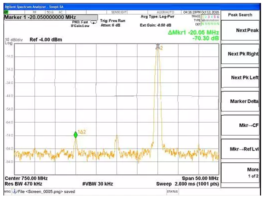
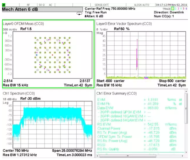
The following are LO and image suppression indicators and TDD-LTEEVM tests (please contact us for more detailed test content)
(1).LO and Image reject performance

Test conditions: single-tone signal mode, the input power of the signal source is -14dBm, and the power output to the spectrum analyzer after the HJX-AD9371-SDR development board is -5dBm.
(2).EVM performance

EVM test conditions: TDD-LTE signal mode, 20MHZ bandwidth, signal source input power is -24dBm, after HJX-AD9371-SDR development board, the power output to the spectrum analyzer is -15dBm.
5.the application scenario:
- Radio repeater station
- Digital fiber repeater station
- 3G/4G microbase stations and acer stations (BTS)
- 3G/4G multicarrier picohoneycomb
- FDD and TDD active antenna systems
- Microwave non-line-of-sight (NLOS) return trip system
- 5 G prototype


